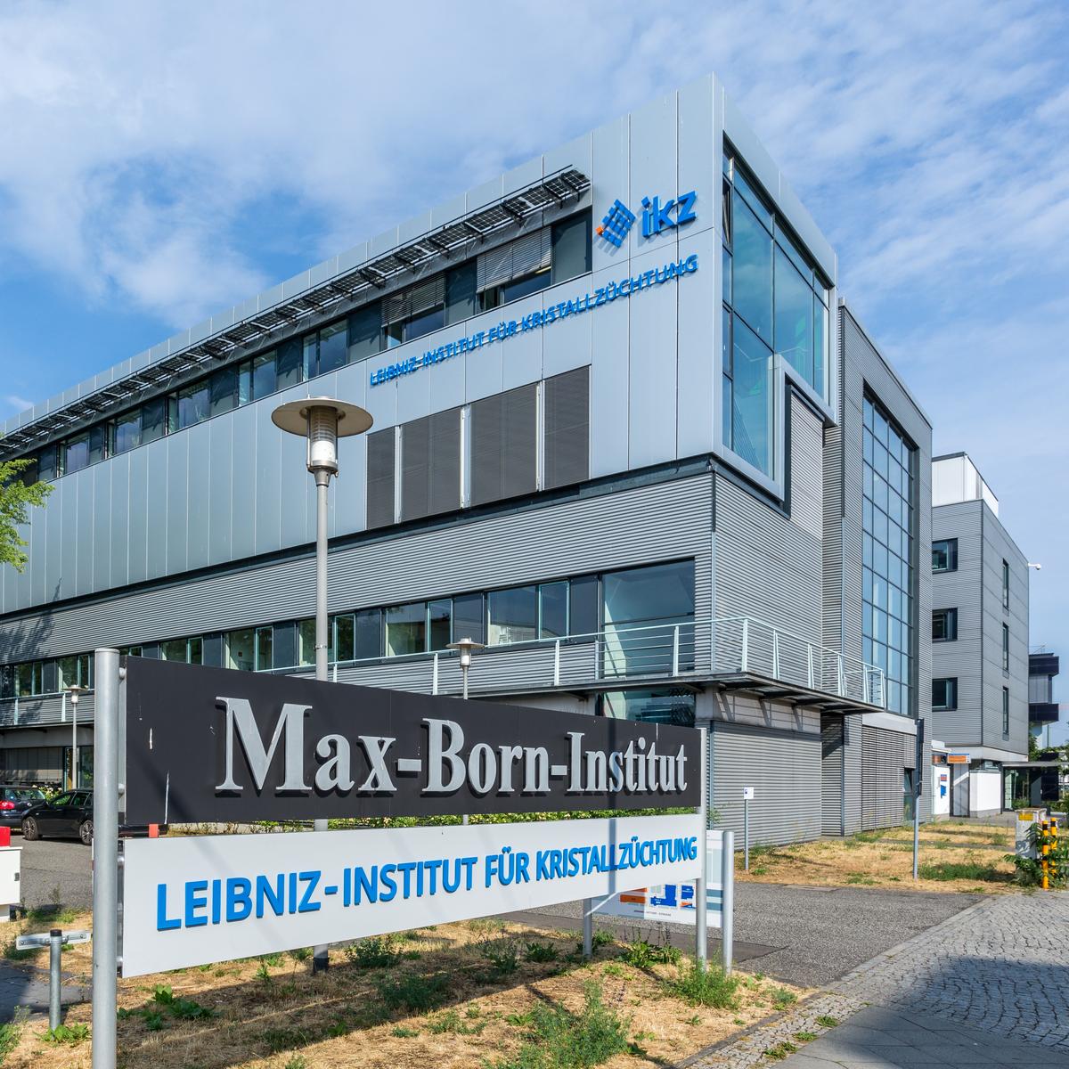
Technological advancement in gallium oxide semiconductor materials
The EFRE project G.O.A.L. (1.6-14) “Gallium Oxide Application Laboratory for Power Electronics”, which was launched in September 2024, completes the value chain created at the IKZ in the field of gallium oxide technology development. In addition to the existing Cz volume crystal growing and wafering sections, the epitaxy module in the form of a 3x2” MOVPE from AIXTRON has now been added. This expansion creates the prerequisite for establishing IKZ in the EU as the only supplier of 2 inch gallium oxide epi-wafers for technology prototyping for research and industry. Over the past three years, IKZ has invested around €5 million in modern equipment along the value chain.
Key material for the energy transition
The development of innovative solutions for efficient power electronics plays a crucial role in connection with the energy transition. The novel semiconductor material gallium oxide has the potential for low-loss and cost-effective power electronics and could therefore make a decisive contribution to such a solution. Co-financed by the European Regional Development Fund (EFRE), the new EFRE application laboratory GOAL to be set up at the IKZ aims to provide gallium oxide epi-wafers with defined and reproducible properties. It is the stable and reliable availability of precise epitaxial wafers that makes subsequent component development possible in the first place. In Japan, Korea and China, there are already government-funded programs to establish a complete process chain for gallium oxide electronics. In the USA, the topic is being developed primarily by the US Air Force. This shows the urgency for Europe and Germany not to lose touch here. The laboratory therefore wants to establish itself as an EU-wide research partner and supplier of 2-inch gallium oxide epitaxial wafers as a base material for components for power electronics. It can draw on a network of research institutions and small and medium-sized enterprises in the Berlin-Brandenburg region; an essential understanding of the material gallium oxide has been developed over many years together with partners in the Leibniz Science Campus 'Growth & Fundamentals of Oxides (Grafox) I & II' under the direction of the Paul Drude Institute (PDI).
New markets enabled by innovative semiconductors
Gallium oxide power electronics addresses various fields of application. New markets are opening up primarily at the level of semiconductor technologies (wafers, transistors, power modules) and through higher added value in the electronics industry with power electronic converters for e-mobility, PV, wind power and power plant conversion, for example. Wafer layer systems with dimensions of at least 2 inches are required to bring the material into application and enable the development of components. For this purpose, with the help of investment funds, the EFRE-GOAL project will be equipped with a suitable industrial level metal-organic vapor phase epitaxy system from AIXTRON. The epitaxy process will be further developed to 2 inches in cooperation with technology developers (e.g. Ferdinand-Braun-Institut Berlin). Volume crystals and their processing are developed and made available by the institute itself with respect to larger diameters, for which the IKZ works in part with other Berlin companies such as CrysTec GmbH, LayTec etc. in this area.
Greater sovereignty for Europe's semiconductor industry
Innovative and disruptive technologies are the key to mastering the challenges of our modern society in terms of energy, mobility, communication, health and climate, etc. New and innovative materials in particular are able to decisively advance these technologies and enable new approaches to solutions. However, the basis for the development of new technologies is the availability of materials with precisely defined and reliably reproducible properties. GOAL will close this gap in the value chain for gallium oxide and thus strengthen the innovative capacity and technological sovereignty of Berlin, Germany and Europe. The results from GOAL will be published with the aim of triggering and strengthening innovation processes in Germany. Due to the high industrial relevance, direct utilization in the semiconductor and power electronics industry (such as BOSCH, Infineon, ZF etc.) is also to be expected. The IKZ start-up “NextGO-Epi”, which was founded in April 2025, will also significantly improve its chances of success with GOAL.
Source: Press release IKZ „Technology development for semiconductor material gallium oxide launched“, 04|15|2025, Link to the Leibniz Institute for Crystal Growth
Renewable Energy Reinvented: The Capital Region Innovation Hub
The capital region of Berlin-Brandenburg is a European hotspot for the development and application of forward-looking energy technologies. With the highest concentration of solar energy research and development in Europe, a strong industrial backbone, and a vibrant start-up scene, technological solutions for the energy transition of tomorrow are being created here. Projects such as the EFRE-GOAL laboratory for gallium oxide epitaxy also demonstrate how targeted investments in new materials and semiconductor technologies can enable the transfer of innovation into real-world applications.
Berlin and Brandenburg offer excellent research institutions, interconnected industrial clusters, and a hands-on environment—ideal conditions for building a resilient and sovereign energy and electronics industry. As Germany’s largest practical testing ground for electromobility and a pioneer in the transition toward renewable energies, the region holds a leading position both nationally and across Europe.
For more information on the sector priorities and support programs for companies, investors and research institutions, please contact us:
Sandra Koletzki | sandra.koletzki(at)airport-region.de
